

In a landmark moment for the semiconductor industry, Intel Corporation (NASDAQ: INTC) has officially announced that its cutting-edge 18A (1.8nm-class) manufacturing node has entered high-volume manufacturing (HVM). This achievement marks the successful completion of CEO Pat Gelsinger’s ambitious "five nodes in four years" (5N4Y) strategy, positioning the company at the forefront of the global race for transistor density and energy efficiency. As of January 1, 2026, the first consumer and enterprise chips built on this process—codenamed Panther Lake and Clearwater Forest—are beginning to reach the market, signaling a new era for AI-driven computing.
The announcement is further bolstered by the release of Process Design Kits (PDKs) for Intel’s next-generation 14A node to external foundry customers. By sharing these 1.4nm-class tools, Intel is effectively inviting the world’s most advanced chip designers to begin building the future of US-based manufacturing. This progress is not merely a corporate milestone; it represents a fundamental shift in the technological landscape, as Intel leverages its first-mover advantage in backside power delivery and gate-all-around (GAA) transistor architectures to challenge the dominance of rivals like TSMC (NYSE: TSM) and Samsung (KRX:005930).
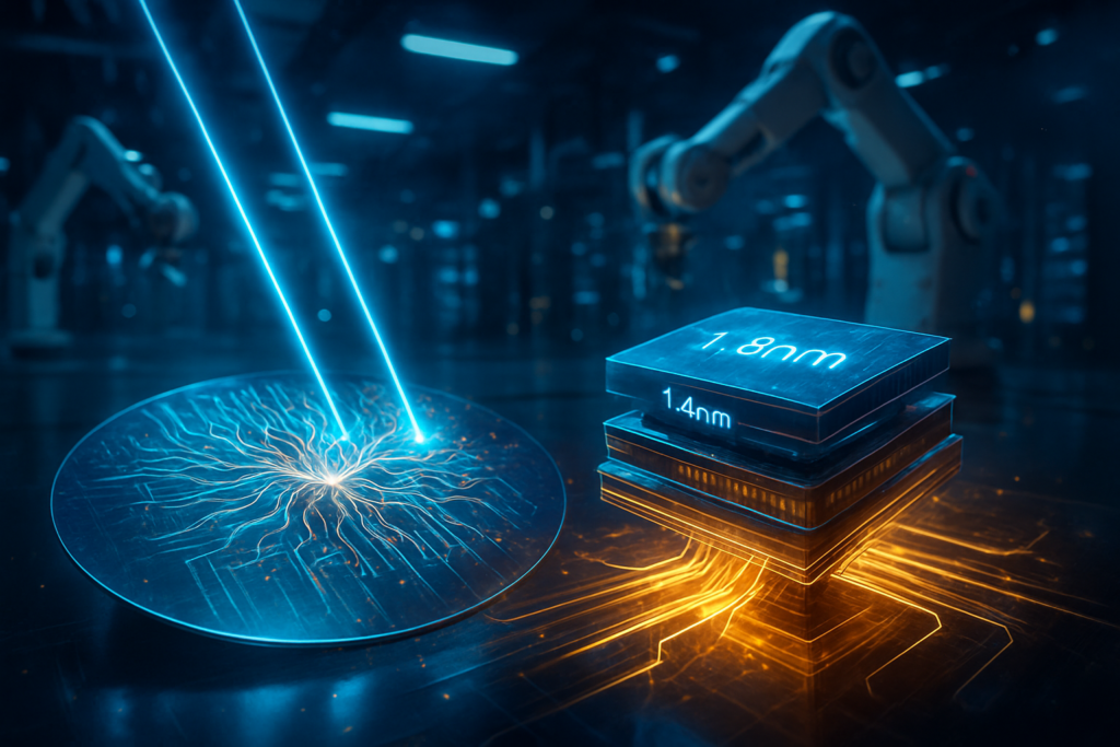
The Architecture of Leadership: RibbonFET, PowerVia, and the 18A-PT Breakthrough
At the heart of Intel’s 18A node are two revolutionary technologies: RibbonFET and PowerVia. RibbonFET is Intel’s implementation of GAA transistors, which replace the long-standing FinFET design to provide better control over the electrical current, reducing leakage and increasing performance. While Samsung was the first to introduce GAA at the 3nm level, Intel’s 18A is the first to pair it with PowerVia—the industry's first functional backside power delivery system. By moving the power delivery circuitry to the back of the silicon wafer, Intel has eliminated the "wiring congestion" that has plagued chip design for decades. This allows for a 5% to 10% increase in logic density and significantly improved power efficiency, a critical factor for the massive power requirements of modern AI data centers.
Intel has also introduced a specialized variant known as 18A-PT (Performance-Tuned). This node is specifically optimized for 3D-integrated circuits (3D IC) and features Foveros Direct 3D hybrid bonding. By reducing the vertical interconnect pitch to less than 5 microns, 18A-PT allows for the seamless stacking of compute dies, such as a 14A processor sitting directly atop an 18A-PT base die. This modular approach to chip design is expected to become the industry standard for high-performance AI accelerators, where memory and compute must be physically closer than ever before to minimize latency.
The technical community has responded with cautious optimism. While early yields for 18A were reported in the 55%–65% range throughout late 2025, the trajectory suggests that Intel will reach commercial-grade maturity by mid-2026. Industry experts note that Intel’s lead in backside power delivery gives them a roughly 18-month headstart over TSMC’s N2P node, which is not expected to integrate similar technology until later this year. This "technological leapfrogging" has placed Intel in a unique position where it is no longer just catching up, but actively setting the pace for the 2nm transition.
The Foundry War: Microsoft, AWS, and the Battle for AI Supremacy
The success of 18A and the early rollout of 14A PDKs have profound implications for the competitive landscape of the tech industry. Microsoft (NASDAQ: MSFT) has emerged as a primary "anchor customer" for Intel Foundry, utilizing the 18A node for its Maia AI accelerators. Similarly, Amazon (NASDAQ: AMZN) has signed a multi-billion dollar agreement to produce custom AWS silicon on Intel's advanced nodes. For these tech giants, the ability to source high-end chips from US-based facilities provides a critical hedge against geopolitical instability in the Taiwan Strait, where the majority of the world's advanced logic chips are currently produced.
For startups and smaller AI labs, the availability of 14A PDKs opens the door to "next-gen" performance that was previously the exclusive domain of companies with deep ties to TSMC. Intel’s aggressive push into the foundry business is disrupting the status quo, forcing TSMC and Samsung to accelerate their own roadmaps. As Intel begins to offer its 14A node—the first in the industry to utilize High-NA (Numerical Aperture) EUV lithography—it is positioning itself as the premier destination for companies building the next generation of Large Language Models (LLMs) and autonomous systems that require unprecedented compute density.
The strategic advantage for Intel lies in its "systems foundry" approach. Unlike traditional foundries that only manufacture wafers, Intel is offering a full stack of services including advanced packaging (Foveros), standardized chiplet interfaces, and software optimizations. This allows customers like Broadcom (NASDAQ: AVGO) and Ericsson to design complex, multi-die systems that are more efficient than traditional monolithic chips. By securing these high-profile partners, Intel is validating its business model and proving that it can compete on both technology and service.
A Geopolitical and Technological Pivot: The 2nm Milestone
The transition to the 2nm class (18A) and beyond (14A) is more than just a shrinking of transistors; it is a critical component of the global AI arms race. As AI models grow in complexity, the demand for "sovereign AI" and domestic manufacturing capabilities has skyrocketed. Intel’s progress is a major win for the US Department of Defense and the RAMP-C program, which seeks to ensure that the most advanced chips for national security are built on American soil. This shift reduces the "single point of failure" risk inherent in the global semiconductor supply chain.
Comparing this to previous milestones, the 18A launch is being viewed as Intel's "Pentium moment" or its return to the "Tick-Tock" cadence that defined its dominance in the 2000s. However, the stakes are higher now. The integration of High-NA EUV in the 14A node represents the most significant change in lithography in over a decade. While there are concerns regarding the astronomical costs of these machines—each costing upwards of $350 million—Intel’s early adoption gives it a learning curve advantage that rivals may struggle to close.
The broader AI landscape will feel the effects of this progress through more efficient edge devices. With 18A-powered laptops and smartphones hitting the market in 2026, "Local AI" will become a reality, allowing complex generative AI tasks to be performed on-device without relying on the cloud. This has the potential to address privacy concerns and reduce the carbon footprint of AI, though it also raises new challenges regarding hardware obsolescence and the rapid pace of technological turnover.
Looking Ahead: The Road to 14A and the High-NA Era
As we look toward the remainder of 2026 and into 2027, the focus will shift from 18A's ramp-up to the risk production of 14A. This node will introduce "PowerDirect," Intel’s second-generation backside power delivery system, which promises even lower resistance and higher performance-per-watt. The industry is closely watching Intel's Oregon and Arizona fabs to see if they can maintain the yield improvements necessary to make 14A a commercial success.
The near-term roadmap also includes the release of 18A-P, a performance-enhanced version of the current flagship node, slated for late 2026. This will likely serve as the foundation for the next generation of high-end gaming GPUs and AI workstations. Challenges remain, particularly in the realm of thermal management as power density continues to rise, and the industry will need to innovate new cooling solutions to keep up with these 1.4nm-class chips.
Experts predict that by 2028, the "foundry landscape" will look entirely different, with Intel potentially holding a significant share of the external manufacturing market. The success of 14A will be the ultimate litmus test for whether Intel can truly sustain its lead. If the company can deliver on its promise of High-NA EUV production, it may well secure its position as the world's most advanced semiconductor manufacturer for the next decade.
Conclusion: The New Silicon Standard
Intel’s successful execution of its 18A and 14A roadmap is a defining chapter in the history of the semiconductor industry. By delivering on the "5 Nodes in 4 Years" promise, the company has silenced many of its skeptics and demonstrated a level of technical agility that few thought possible just a few years ago. The combination of RibbonFET, PowerVia, and the early adoption of High-NA EUV has created a formidable technological moat that positions Intel as a leader in the AI era.
The significance of this development cannot be overstated; it marks the return of leading-edge manufacturing to the United States and provides the hardware foundation necessary for the next leap in artificial intelligence. As 18A chips begin to power the world’s data centers and personal devices, the industry will be watching closely for the first 14A test chips. For now, Intel has proven that it is back in the game, and the race for the sub-1nm frontier has officially begun.
This content is intended for informational purposes only and represents analysis of current AI developments.
TokenRing AI delivers enterprise-grade solutions for multi-agent AI workflow orchestration, AI-powered development tools, and seamless remote collaboration platforms.
For more information, visit https://www.tokenring.ai/.