

In a move that signals a paradigm shift for the semiconductor industry, Austin-based startup Neurophos has announced the closing of a $110 million Series A funding round to commercialize its breakthrough metamaterial-based photonic AI chips. Led by Gates Frontier, the venture arm of Bill Gates, the funding marks a massive bet on the future of optical computing as traditional silicon-based processors hit the "thermal wall" of physics. By utilizing light instead of electricity for computation, Neurophos aims to deliver a staggering 100x improvement in energy efficiency and processing speed compared to today’s leading graphics processing units (GPUs).
The investment arrives at a critical juncture for the AI industry, where the energy demands of massive Large Language Models (LLMs) have begun to outstrip the growth of power grids. As tech giants scramble for ever-larger clusters of NVIDIA (NASDAQ: NVDA) H100 and Blackwell chips, Neurophos promises a "drop-in replacement" that can handle the massive matrix-vector multiplications of AI inference at the speed of light. This Series A round, which includes strategic participation from Microsoft (NASDAQ: MSFT) via its M12 fund and Saudi Aramco (TADAWUL: 2222), positions Neurophos as the primary challenger to the electronic status quo, moving the industry toward a post-Moore’s Law era.
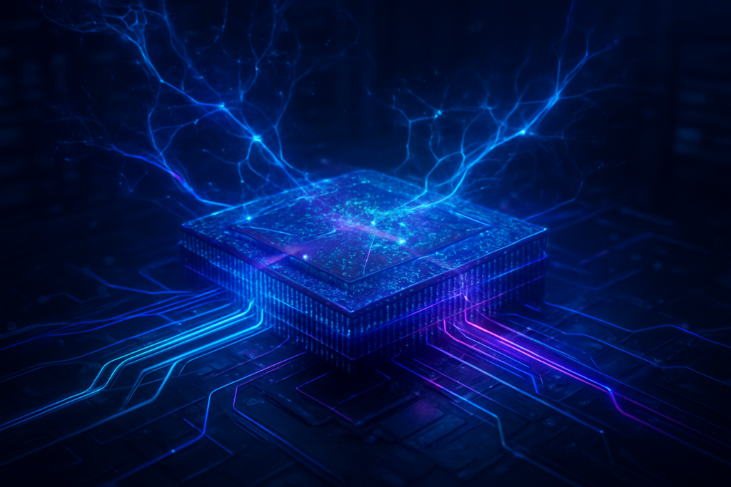
The Metamaterial Breakthrough: 56 GHz and Micron-Scale Optical Transistors
At the heart of the Neurophos breakthrough is a proprietary Optical Processing Unit (OPU) known as the Tulkas T100. Unlike previous attempts at optical computing that relied on bulky silicon photonics components, Neurophos utilizes micron-scale metasurface modulators. These "metamaterials" are effectively 10,000 times smaller than traditional photonic modulators, allowing the company to pack over one million processing elements onto a single device. This extreme density enables the creation of a 1,000×1,000 optical tensor core, dwarfing the 256×256 matrices found in the most advanced electronic architectures.
Technically, the Tulkas T100 operates at an unprecedented clock frequency of 56 GHz—more than 20 times the boost clock of current flagship GPUs from NVIDIA (NASDAQ: NVDA) or Intel (NASDAQ: INTC). Because the computation occurs as light passes through the metamaterial, the chip functions as a "fully in-memory" processor. This eliminates the "von Neumann bottleneck," where data must constantly be moved between the processor and memory, a process that accounts for up to 90% of the energy consumed by traditional AI chips. Initial benchmarks suggest the Tulkas T100 can achieve 470 PetaOPS of throughput, a figure that dwarfs even the most optimistic projections for upcoming electronic platforms.
The industry's reaction to the Neurophos announcement has been one of cautious optimism mixed with technical awe. While optical computing has long been dismissed as "ten years away," the ability of Neurophos to manufacture these chips using standard CMOS processes at foundries like Taiwan Semiconductor Manufacturing Company (NYSE: TSM) is a significant differentiator. Researchers note that by avoiding the need for specialized manufacturing equipment, Neurophos has bypassed the primary scaling hurdle that has plagued other photonics startups. "We aren't just changing the architecture; we're changing the medium of thought for the machine," noted one senior researcher involved in the hardware validation.
Disrupting the GPU Hegemony: A New Threat to Data Center Dominance
The $110 million infusion provides Neurophos with the capital necessary to begin mass production and challenge the market dominance of established players. Currently, the AI hardware market is almost entirely controlled by NVIDIA (NASDAQ: NVDA), with companies like Advanced Micro Devices (NASDAQ: AMD) and Alphabet Inc. (NASDAQ: GOOGL) through its TPUs trailing behind. However, the sheer energy efficiency of the Tulkas T100—estimated at 300 to 350 TOPS per watt—presents a strategic advantage that electronic chips cannot match. For hyperscalers like Microsoft (NASDAQ: MSFT) and Amazon (NASDAQ: AMZN), transitioning to photonic chips could reduce data center power bills by billions of dollars annually.
Strategically, Neurophos is positioning its OPU as a "prefill processor" for LLM inference. In the current AI landscape, the "prefill" stage—where the model processes an initial prompt—is often the most compute-intensive part of the cycle. By offloading this task to the Tulkas T100, data centers can handle thousands of more tokens per second without increasing their carbon footprint. This creates a competitive "fork in the road" for major AI labs like OpenAI and Anthropic: continue to scale with increasingly inefficient electronic clusters or pivot toward a photonic-first infrastructure.
The participation of Saudi Aramco (TADAWUL: 2222) and Bosch Ventures in this round also hints at the geopolitical and industrial implications of this technology. With global energy security becoming a primary concern for AI development, the ability to compute more while consuming less is no longer just a technical advantage—it is a sovereign necessity. If Neurophos can deliver on its promise of a "drop-in" server tray, the current backlog for high-end GPUs could evaporate, fundamentally altering the market valuation of the "Magnificent Seven" tech giants who have bet their futures on silicon.
A Post-Silicon Future: The Sustainability of the AI Revolution
The broader significance of the Neurophos funding extends beyond corporate balance sheets; it addresses the growing sustainability crisis facing the AI revolution. As of 2026, data centers are projected to consume a significant percentage of the world's electricity. The "100x efficiency" claim of photonic integrated circuits (PICs) offers a potential escape hatch from this environmental disaster. By replacing heat-generating electrons with cool-running photons, Neurophos effectively decouples AI performance from energy consumption, allowing models to scale to trillions of parameters without requiring their own dedicated nuclear power plants.
This development mirrors previous milestones in semiconductor history, such as the transition from vacuum tubes to transistors or the birth of the integrated circuit. However, unlike those transitions which took decades to mature, the AI boom is compressing the adoption cycle for photonic computing. We are witnessing the exhaustion of traditional Moore’s Law, where shrinking transistors further leads to leakage and heat that cannot be managed. Photonic chips like those from Neurophos represent a "lateral shift" in physics, moving the industry onto a new performance curve that could last for the next fifty years.
However, challenges remain. The industry has spent forty years optimizing software for electronic architectures. To succeed, Neurophos must prove that its full software stack is truly compatible with existing frameworks like PyTorch and TensorFlow. While the company claims its chips are "software-transparent," the history of alternative hardware is littered with startups that failed because developers found their tools too difficult to use. The $110 million investment will be largely directed toward ensuring that the transition from NVIDIA (NASDAQ: NVDA) CUDA-based workflows to Neurophos’ optical environment is as seamless as possible.
The Road to 2028: Mass Production and the Optical Roadmap
Looking ahead, Neurophos has set a roadmap that targets initial commercial deployment and early-access developer hardware throughout 2026 and 2027. Volume production is currently slated for 2028. During this window, the company must bridge the gap from validated prototypes to the millions of units required by global data centers. The near-term focus will likely be on specialized AI workloads, such as real-time language translation, high-frequency financial modeling, and complex scientific simulations, where the 56 GHz clock speed provides an immediate, unmatchable edge.
Experts predict that the next eighteen months will see a "gold rush" in the photonics space, as competitors like Lightmatter and Ayar Labs feel the pressure to respond to the Neurophos metamaterial advantage. We may also see defensive acquisitions or partnerships from incumbents like Intel (NASDAQ: INTC) or Cisco Systems (NASDAQ: CSCO) as they attempt to integrate optical interconnects and processing into their own future roadmaps. The primary hurdle for Neurophos will be the "yield" of their 1,000×1,000 matrices—maintaining optical coherence across such a massive array is a feat of engineering that will be tested as they scale toward mass manufacturing.
As the Tulkas T100 moves toward the market, we may also see the emergence of "hybrid" data centers, where electronic chips handle general-purpose tasks while photonic OPUs manage the heavy lifting of AI tensors. This tiered architecture would allow enterprises to preserve their existing investments while gaining the benefits of light-speed inference. If the performance gains hold true in real-world environments, the "electronic era" of AI hardware may be remembered as merely a prologue to the photonic age.
Summary of a Computing Revolution
The $110 million Series A for Neurophos is more than a successful fundraising event; it is a declaration that the era of the electron in high-performance AI is nearing its end. By leveraging metamaterials to shrink optical components to the micron scale, Neurophos has solved the density problem that once made photonic computing a laboratory curiosity. The resulting 100x efficiency gain offers a path forward for an AI industry currently gasping for breath under the weight of its own power requirements.
In the coming weeks and months, the tech world will be watching for the first third-party benchmarks of the Tulkas T100 hardware. The involvement of heavyweight investors like Bill Gates and Microsoft (NASDAQ: MSFT) suggests that the due diligence has been rigorous and the technology is ready for its close-up. If Neurophos succeeds, the geography of the tech industry may shift from the silicon of California to the "optical valleys" of the future. For now, the message is clear: the future of artificial intelligence is moving at the speed of light.
This content is intended for informational purposes only and represents analysis of current AI developments.
TokenRing AI delivers enterprise-grade solutions for multi-agent AI workflow orchestration, AI-powered development tools, and seamless remote collaboration platforms.
For more information, visit https://www.tokenring.ai/.