
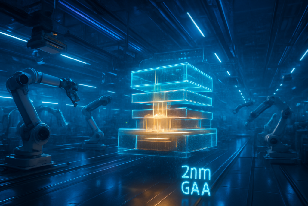
The semiconductor landscape reached a historic milestone this month as Taiwan Semiconductor Manufacturing Company (NYSE: TSM) officially commenced high-volume production of its 2-nanometer (N2) process technology. As of January 14, 2026, the transition represents the most significant architectural overhaul in the company's history, moving away from the long-standing FinFET design to the highly anticipated Gate-All-Around (GAA) nanosheet transistors. This shift is not merely an incremental upgrade; it is a fundamental reconfiguration of the transistor itself, designed to meet the insatiable thermal and computational demands of the generative AI era.
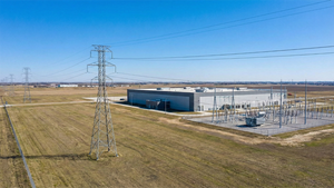
The commencement of N2 volume production arrives at a critical juncture for the global tech economy. With demand for AI hardware continuing to outpace supply, the efficiency gains promised by the 2nm node are expected to redefine the performance ceilings of data centers and consumer devices alike. Production is currently ramping up at TSMC’s state-of-the-art Gigafabs, specifically Fab 20 in Hsinchu and Fab 22 in Kaohsiung. Initial reports from supply chain analysts suggest that yield rates have already stabilized at an impressive 70%, signaling a smooth rollout that could provide TSMC with a decisive advantage over its closest competitors in the sub-3nm race.
Engineering the Future of the Transistor
The technical heart of the N2 node is the transition from FinFET (Fin Field-Effect Transistor) to GAA nanosheet architecture. For over a decade, FinFET served as the industry standard, utilizing a 3D "fin" to control current flow. However, as transistors shrunk toward the physical limits of silicon, FinFETs began to suffer from increased current leakage and thermal instability. The new GAA nanosheet design resolves these bottlenecks by wrapping the gate around the channel on all four sides. This 360-degree contact provides superior electrostatic control, allowing for a 10% to 15% increase in speed at the same power level, or a massive 25% to 30% reduction in power consumption at the same clock speed when compared to the existing 3nm (N3E) process.
Logistically, the rollout is being spearheaded by a "dual-hub" production strategy. Fab 20 in Hsinchu’s Baoshan district was the first to receive 2nm equipment, but it is Fab 22 in Kaohsiung that has achieved the earliest high-volume throughput. These facilities are the most advanced manufacturing sites on the planet, utilizing the latest generation of Extreme Ultraviolet (EUV) lithography to print features so small they are measured in atoms. This density increase—roughly 15% over the 3nm node—allows chip designers to pack more logic and memory into the same physical footprint, a necessity for the multi-billion parameter models that power modern AI.
Initial reactions from the semiconductor research community have been overwhelmingly positive, particularly regarding the power efficiency metrics. Industry experts note that the 30% power reduction is the single most important factor for the next generation of mobile processors. By slashing the energy required for basic logic operations, TSMC is enabling "Always-On" AI features in smartphones that would have previously decimated battery life. Furthermore, the GAA transition allows for finer voltage tuning, giving engineers the ability to optimize chips for specific workloads, such as real-time language translation or complex video synthesis, with unprecedented precision.
The Scramble for Silicon: Apple and NVIDIA Lead the Pack
The immediate business implications of the 2nm launch are profound, as the world’s largest tech entities have already engaged in a bidding war for capacity. Apple (NASDAQ: AAPL) has reportedly secured over 50% of TSMC's initial N2 output for 2026. This silicon is destined for the upcoming A20 Pro chips, which are expected to power the iPhone 18 series, as well as the M6 family of processors for the Mac and iPad. For Apple, the N2 node is the key to localizing "Apple Intelligence" more deeply into its hardware, reducing the reliance on cloud-based processing and enhancing user privacy through on-device execution.
Following closely behind is NVIDIA (NASDAQ: NVDA), which has pivoted its roadmap to utilize 2nm for its next-generation AI architectures, codenamed "Rubin Ultra" and "Feynman." As AI models grow in complexity, the heat generated by data centers has become a primary bottleneck for scaling. NVIDIA’s move to 2nm is strategically aimed at the 25-30% power reduction, which will allow data center operators to increase compute density without requiring a proportional increase in cooling infrastructure. This transition places NVIDIA in an even stronger position to maintain its dominance in the AI accelerator market, as its competitors scramble to find comparable manufacturing capacity.
The competitive landscape remains fierce, as Intel (NASDAQ: INTC) and Samsung (KRX: 005930) are also vying for the 2nm crown. Intel’s 18A process, which achieved volume production in late 2025, has introduced "PowerVia" backside power delivery—a technology TSMC will not implement until its N2P node later this year. While Intel currently holds a slight lead in power delivery architecture, TSMC’s N2 holds a significant advantage in transistor density and yield stability. Meanwhile, Samsung is positioning its SF2 process as a cost-effective alternative for companies like Qualcomm (NASDAQ: QCOM) and MediaTek (TWSE: 2454), who are looking to avoid the premium $30,000-per-wafer price tag associated with TSMC’s first-run 2nm capacity.
Reimagining Moore’s Law in the Age of AI
The commencement of 2nm production marks a pivotal moment in the broader AI landscape. For years, critics have argued that Moore’s Law—the observation that the number of transistors on a microchip doubles roughly every two years—was reaching its physical end. The successful implementation of GAA nanosheets at 2nm proves that through radical architectural shifts, performance scaling can continue. This milestone is not just about making chips faster; it is about the "sustainability of scale" for AI. By drastically reducing the power-per-operation, TSMC is providing the foundational infrastructure needed to transition AI from a niche cloud service to an omnipresent utility embedded in every piece of hardware.
However, the transition also brings significant concerns regarding the centralization of the AI supply chain. With TSMC being the only foundry currently capable of delivering high-yield 2nm GAA wafers at this scale, the global AI economy remains heavily dependent on a single company and a single geographic region. This concentration has sparked renewed discussions about the resilience of the global chip industry and the necessity of regional chip acts to diversify manufacturing. Furthermore, the skyrocketing costs of 2nm development—estimated at billions of dollars in R&D and equipment—threaten to widen the gap between tech giants who can afford the latest silicon and smaller startups that may be left using older, less efficient hardware.
When compared to previous milestones, such as the 7nm transition in 2018 or the 5nm launch in 2020, the 2nm era feels fundamentally different. While previous nodes focused on general-purpose compute, N2 has been engineered from the ground up with AI workloads in mind. The integration of high-bandwidth memory (HBM) and advanced packaging techniques like CoWoS (Chip on Wafer on Substrate) alongside the 2nm logic die represents a shift from "system-on-chip" to "system-in-package," where the transistor is just one part of a much larger, interconnected AI engine.
The Roadmap to 1.6nm and Beyond
Looking ahead, the 2nm launch is merely the beginning of an aggressive multi-year roadmap. TSMC has already confirmed that an enhanced version of the process, N2P, will arrive in late 2026. N2P will introduce Backside Power Delivery (BSPD), a feature that moves power routing to the rear of the wafer to reduce interference and further boost efficiency. This will be followed closely by the A16 node, often referred to as "1.6nm," which will incorporate "Super Power Rail" technology and potentially the first widespread use of High-NA EUV lithography.
In the near term, we can expect a flurry of product announcements throughout 2026 as the first 2nm-powered devices hit the market. The industry will be watching closely to see if the promised 30% power savings translate into real-world battery life gains and more capable generative AI assistants. The next major hurdle for TSMC and its partners will be the transition to even more exotic materials, such as 2D semiconductors and carbon nanotubes, which are currently in the early research phases at TSMC’s R&D centers in Hsinchu.
Experts predict that the success of the 2nm node will dictate the pace of AI innovation for the remainder of the decade. If yield rates continue to improve and the GAA architecture proves reliable in the field, it will pave the way for a new generation of "Super-AI" chips that could eventually achieve human-level reasoning capabilities in a form factor no larger than a credit card. The challenges of heat dissipation and power delivery remain significant, but with the 2nm era now officially underway, the path forward for high-performance silicon has never been clearer.
A New Benchmark for the Silicon Age
The official start of 2nm volume production at TSMC is more than just a win for the Taiwanese foundry; it is a vital heartbeat for the global technology industry. By successfully navigating the transition from FinFET to GAA, TSMC has secured its role as the primary architect of the hardware that will define the late 2020s. The 10-15% speed gains and 25-30% power reductions are the fuel that will drive the next wave of AI breakthroughs, from autonomous robotics to personalized medicine.
As we look back at this moment in semiconductor history, the launch of N2 will likely be remembered as the point where "AI-native silicon" became the standard. The immense complexity of manufacturing at this scale highlights the specialized expertise required to keep the wheels of modern civilization turning. While the geopolitical and economic stakes of chip manufacturing continue to rise, the technical achievement of 2nm volume production stands as a testament to human ingenuity and the relentless pursuit of efficiency.
In the coming weeks and months, the tech world will be monitoring the first commercial shipments of 2nm wafers. Success will be measured not just in transistor counts, but in the performance of the devices in our pockets and the servers in our data centers. As the first GAA nanosheet chips begin their journey from the cleanrooms of Kaohsiung to the palms of consumers worldwide, the 2nm era has officially arrived, and with it, the next chapter of the digital revolution.
This content is intended for informational purposes only and represents analysis of current AI developments.
TokenRing AI delivers enterprise-grade solutions for multi-agent AI workflow orchestration, AI-powered development tools, and seamless remote collaboration platforms.
For more information, visit https://www.tokenring.ai/.