

TORRANCE, Calif., May 05, 2025 (GLOBE NEWSWIRE) -- Navitas Semiconductor (Nasdaq: NVTS), the only pure-play, next-generation power semiconductor company and industry leader in gallium nitride (GaN) power ICs and silicon carbide (SiC) technology, introduces a new level of reliability to meet the system lifetime requirements of the most demanding automotive and industrial applications. Navitas’ latest generation of 650 V and 1200 V ‘trench-assisted planar’ SiC MOSFETs combined with an optimized, HV-T2Pak top-side cooled package, delivers the industry’s highest creepage of 6.45 mm to meet IEC-compliance for applications up to 1200V.
Navitas’ HV-T2Pak SiC MOSFETs significantly increase system-level power density and efficiency while improving thermal management and simplifying board-level design and manufacturability. Target applications include EV on-board chargers (OBC) & DC-DC converters, data-center power supplies, residential solar inverters & energy storage systems (ESS), EV DC fast chargers, and HVAC motor drives.
AEC-Q101 is an automotive industry standard developed by the Automotive Electronics Council (AEC) to establish common part-qualification and quality-system standards. Navitas has created an industry-first benchmark, ‘AEC-Plus’*, indicating parts qualified above and beyond the existing AEC-Q101 and JEDEC product qualification standards. This new benchmark showcases Navitas’ deep understanding of system-level lifetime requirements and a strong commitment to enabling rigorously designed and validated products for demanding mission profiles in automotive and industrial applications.
The ‘AEC-Plus’ qualification standards extend further into rigorous multi-lot testing and qualification. Key additions to the existing AEC-Q101 requirements include:
- Dynamic reverse bias (D-HTRB) & dynamic gate switching (D-HTGB) to represent stringent application mission profiles
- Over 2x longer power & temperature cycling
- Over 3x longer duration for static high-temperature, high-voltage tests (e.g. HTRB, HTGB)
- 200°C TJMAX qualification for overload operation capability
Navitas’ HV-T2Pak top-side cooled package, in an industry-standard compact form factor (14 mm x 18.5 mm), is optimized with an innovative groove design in the package mold compound that extends the creepage to 6.45 mm without reducing the size of the exposed thermal pad and ensuring optimal heat dissipation.
In addition, the exposed thermal pad has a nickel, nickel-phosphorus (NiNiP) plating, as opposed to tin (Sn) plating from existing TSC package solutions, which is critical to preserving the post-reflow surface planarity of the exposed pad and ensuring thermally efficient and reliable attachment to the thermal interface material (TIM).
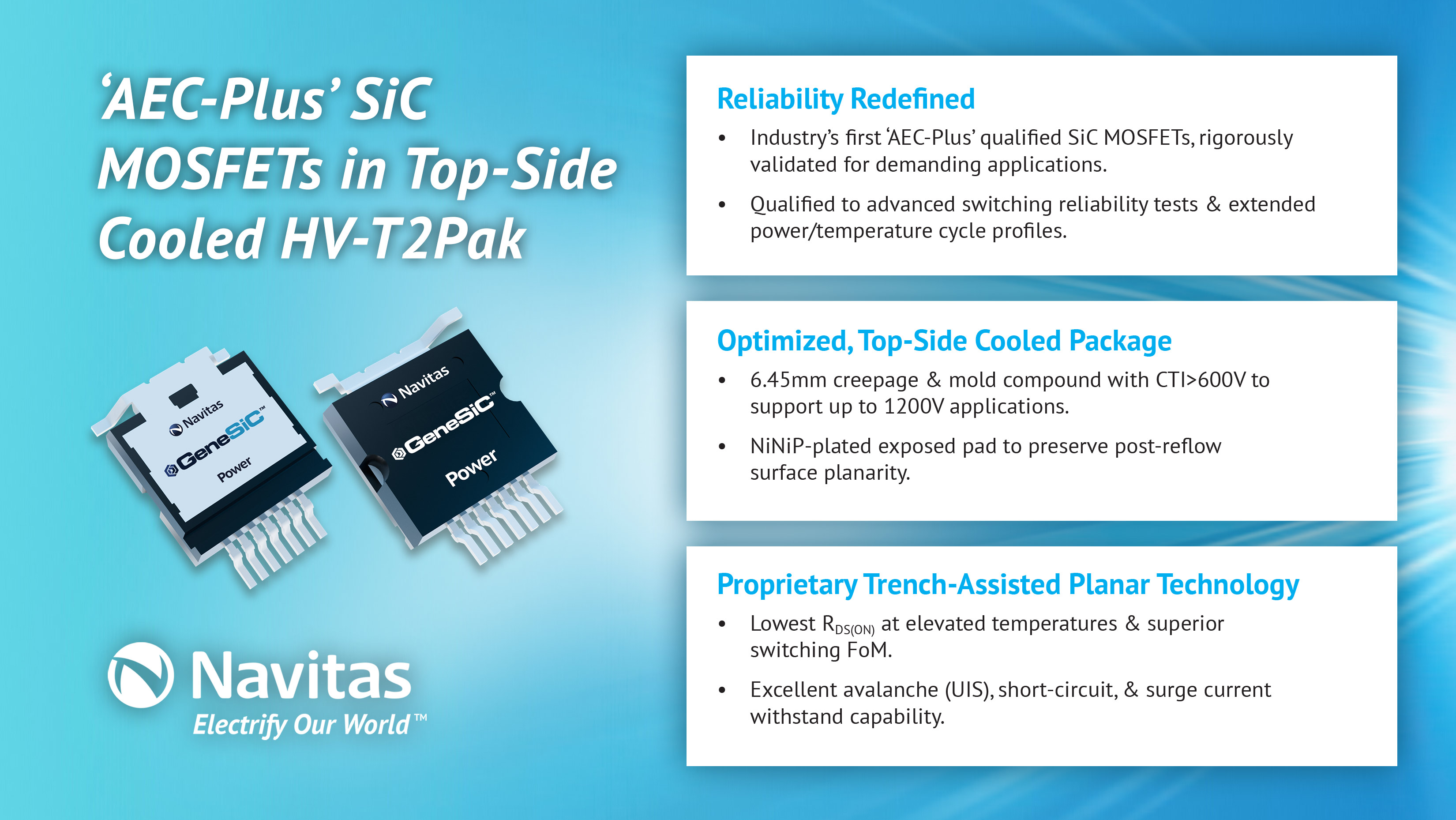
Enabled by over 20 years of SiC technology innovation leadership, Navitas’ GeneSiC™ ‘trench-assisted planar SiC MOSFET technology’ offers up to 20% lower on-resistance under in-circuit operation at high temperatures compared to competition and superior switching figure-of-merits which result in the lowest power losses across a wider operating range. All GeneSiC™ SiC MOSFETs have the highest-published 100%-tested avalanche capability, excellent short-circuit withstand energy, and tight threshold voltage distributions for easy paralleling.
The initial HV-T2Pak portfolio includes 1200 V SiC MOSFETs with on-resistance ratings ranging from 18 mΩ to 135 mΩ and 650 V SiC MOSFETs with on-resistance ratings ranging from 20 mΩ to 55 mΩ. Lower on-resistance (<15 mΩ) SiC MOSFETs in HV-T2Pak package will be announced later in 2025.
For more information, please contact info@navitassemi.com or visit www.navitassemi.com
*Navitas uses the term ‘AEC-Plus’ to indicate parts exceeding AEC-Q101 standards for reliability testing, published by the Automotive Electronics Council (AEC), based on Navitas test results
About Navitas
Navitas Semiconductor (Nasdaq: NVTS) is the only pure-play, next-generation power-semiconductor company, celebrating 10 years of power innovation founded in 2014. GaNFast™ power ICs integrate gallium nitride (GaN) power and drive, with control, sensing, and protection to enable faster charging, higher power density, and greater energy savings. Complementary GeneSiC™ power devices are optimized high-power, high-voltage, and high-reliability silicon carbide (SiC) solutions. Focus markets include AI data centers, EV, solar, energy storage, home appliance / industrial, mobile, and consumer. Over 300 Navitas patents are issued or pending, with the industry’s first and only 20-year GaNFast warranty. Navitas was the world’s first semiconductor company to be CarbonNeutral®-certified.
Navitas Semiconductor, GaNFast, GaNSense, GeneSiC, and the Navitas logo are trademarks or registered trademarks of Navitas Semiconductor Limited and affiliates. All other brands, product names, and marks are or may be trademarks or registered trademarks used to identify products or services of their respective owners.
Contact Information
Llew Vaughan-Edmunds, Sr Director, Product Management & Marketing
info@navitassemi.com
Photos accompanying this announcement are available at:
https://www.globenewswire.com/NewsRoom/AttachmentNg/57183cfd-fedb-4762-89e2-0e241d5bd56e
https://www.globenewswire.com/NewsRoom/AttachmentNg/d220b5fc-9a6e-46dc-81f2-b4d09ed390c4

![]()