

TORRANCE, Calif., Oct. 13, 2025 (GLOBE NEWSWIRE) -- Navitas Semiconductor (Nasdaq: NVTS), the industry leader in next-generation GaNFast™ gallium nitride (GaN) and GeneSiC™ silicon carbide (SiC) power semiconductors, announced progress in its development of advanced medium and high 800 VDC voltage GaN and SiC power devices to enable the 800 VDC power architecture announced by NVIDIA for next-generation AI factory computing platforms.
With the emergence of the ‘AI factory’, a new class of data center purpose-built for large-scale, synchronous AI and high-performance computing (HPC) workloads, has introduced a set of power challenges. Traditional enterprise and cloud data centers, which rely on legacy 54 V in-rack power distribution, are unable to longer meet the multi-megawatt rack densities required by today’s accelerated computing platforms. These challenges call for a fundamental architectural shift.
800 VDC power distribution provides:
- Higher efficiency by reducing resistive losses and copper usage
- Scalable infrastructure to deliver MW-scale rack power with highly compact solutions
- Global alignment with the IEC’s low-voltage DC (LVDC) classification (≤1,500 VDC)
- Simplified power distribution with efficient thermal management
The 800 VDC architecture enables direct conversion from 13.8 kVAC utility power to 800 VDC within the data center power room or perimeter. By leveraging solid-state transformers (SSTs) and industrial-grade rectifiers, this approach eliminates multiple traditional AC/DC and DC/DC conversion stages, maximizing energy efficiency, reducing losses, and improving overall system reliability.
The 800 VDC distribution directly powers IT racks, eliminating the need for additional AC-DC conversion stages, and is stepped down through two high-efficiency DC-DC stages (800 VDC to 54 V/12 VDC, and then to point-of-load GPU voltages), to drive advanced infrastructure such as the NVIDIA Rubin Ultra platform.
These state-of-the-art AI factories demand unprecedented levels of power density, efficiency, and scalability, which can be enabled by Navitas’ high-performance GaNFast and GeneSiC technologies.
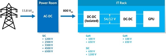
Fig. 1. From the grid to the GPU, Navitas’ advanced GaN and SiC technologies power every stage of the AI data center.
As a pure-play wide bandgap power semiconductor company, Navitas delivers breakthrough GaN and SiC technologies that enable high-efficiency and high-power density power conversion across every stage of the AI data center, from the utility grid to the GPU.
Navitas’ new 100 V GaN FET portfolio delivers superior efficiency, power density, and thermal performance in advanced dual-sided cooled packages. These FETs are specifically optimized for the lower-voltage DC-DC stages on GPU power boards, where ultra-high density and thermal management are critical to meet the demands of next-generation AI compute platforms. Samples, datasheets, and evaluation boards are available for qualified customers.
Additionally, these high efficiency 100V GaN FETs are fabricated on a 200 mm GaN-on-Si process through a new strategic partnership with Power Chip, enabling scalable, high-volume manufacturing.
Navitas’ 650 V GaN portfolio includes a new line of high-power GaN FETs, alongside advanced GaNSafe™ power ICs, which integrate control, drive, sensing, and built-in protection features. This ensures exceptional robustness and reliability, supporting the demanding performance and safety requirements of next-generation AI infrastructure.
GaNSafe™ is the world’s safest GaN platform, featuring ultra-fast short-circuit protection (maximum 350 ns response), 2 kV ESD protection on all pins, elimination of negative gate drive, and programmable slew-rate control. All these features are controlled with 4-pins, allowing the package to be treated like a discrete GaN FET, requiring no VCC pin.
Enabled by over 20 years of SiC innovation leadership, GeneSiC™ proprietary ‘trench-assisted planar’ provides exceptional performance over temperature, delivering high-speed, cool-running operation for high-power, high-reliability applications. GeneSiC technology offers the industry’s broadest voltage range, stretching from 650 V to 6,500 V and has been implemented in multiple megawatt-scale energy storage and grid-tied inverter projects, including collaborations with the U.S. Department of Energy (DoE).
“As NVIDIA drives transformation in AI infrastructure, we’re proud to support this shift with advanced GaN and SiC power solutions that enable the efficiency, scalability, and reliability required by next-generation data centers,” said Chris Allexandre, President and CEO of Navitas. “As the industry moves rapidly toward megawatt-scale AI computing platforms, the need for more efficient, scalable, and reliable power delivery becomes absolutely critical. The transition from legacy 54 V architectures to 800 VDC is not just evolutionary, it’s transformational.”
“Navitas is undergoing a fundamental transformation, driven by the convergence of GaN and SiC technologies to power the world’s most advanced systems. From grid to GPU, our focus now extends far beyond mobile, as we address the megawatt-scale demands of AI factories, smart energy infrastructure, and industrial platforms with differentiated, high-performance power solutions.”
For more information, samples, datasheets, and evaluation boards on Navitas’ latest 100 V and 650 V GaN FETs, as well as our high voltage SiC MOSFET portfolio, please contact info@navitassemi.com.
Read more on Navitas’ Whitepaper on “Redefining Data Center Power: GaN and SiC Technologies for Next-Gen 800 VDC Infrastructure”.
About Navitas
Navitas Semiconductor (Nasdaq: NVTS) is a next-generation power semiconductor leader in gallium nitride (GaN) and IC integrated devices, and high-voltage silicon carbide (SiC) technology, driving innovation across AI and data centers, energy and grid infrastructure, power-performance computing, and industrial applications. With more than 30 years of combined expertise in wide bandgap technologies, GaNFast™ power ICs integrate GaN power, drive, control, sensing, and protection, delivering faster power delivery, higher system density, and greater efficiency. GeneSiC™ high-voltage SiC devices leverage patented trench-assisted planar technology to provide industry-leading voltage capability, efficiency, and reliability for medium-voltage grid and infrastructure applications. Navitas has over 300 patents issued or pending and is the world’s first semiconductor company to be CarbonNeutral®-certified.
Navitas Semiconductor, GaNFast, GaNSense, GeneSiC and the Navitas logo are trademarks or registered trademarks of Navitas Semiconductor Limited and affiliates. All other brands, product names and marks are or may be trademarks or registered trademarks used to identify products or services of their respective owners.
Contact Information
Llew Vaughan-Edmunds, Sr Director, Product Management & Marketing
info@navitassemi.com
Lori Barker, Investor Relations
ir@navitassemi.com
Cautionary Statement Regarding Forward-Looking Statements
This press release and the materials referenced herein include “forward-looking statements” within the meaning of the Securities Exchange Act of 1934, as amended. Other forward-looking statements may be identified by the use of words such as “we expect” or “are expected to be,” “estimate,” “plan,” “project,” “forecast,” “intend,” “anticipate,” “believe,” “seek,” or other similar expressions that predict or indicate future events or trends or that are not statements of historical matters. Forward-looking statements are made based on estimates and forecasts of financial and performance metrics, projections of market opportunity and market share and current indications of customer interest, all of which are based on various assumptions, whether or not identified in this press release. All such statements are based on current expectations and understandings of the management of Navitas and are not predictions of actual future performance. Forward-looking statements are provided for illustrative purposes only and are not intended to serve as, and must not be relied on by any investor as, a guarantee, an assurance, a prediction or a definitive statement of fact or probability. Actual events and circumstances are difficult or impossible to predict and will differ from assumptions and expectations. Many actual events and circumstances that affect performance are beyond the control of Navitas, and forward-looking statements are subject to a number of risks and uncertainties. For example, although our statements in this press release about the development of markets and the potential performance and demand for GaN and SiC power semiconductor products in AI data centers are based on research and analyses which we believe are reasonable, these statements are subject to significant uncertainties, particularly as our products are designed to disrupt existing markets and create new markets. Unlike established markets, such as those for legacy silicon solutions, where historical trends offer some predictive value, new markets present unique challenges and uncertainties.
Photos accompanying this announcement are available at:
https://www.globenewswire.com/NewsRoom/AttachmentNg/e55848b0-7374-49cc-899c-e764de5c8586
https://www.globenewswire.com/NewsRoom/AttachmentNg/c9c34798-d01c-4656-85b1-c780bb28d57e

![]()